
Join 60,000+ competitive exam aspirants
or with email
Your Cart
Subtotal₹0
Total₹0
Examoogle • User • info@examoogle.com • EE-2024-8821
Chapter 1 of 12 • Page 1 of 248🔒 Protected PDF • Watermarked
Join 60,000+ competitive exam aspirants
In the given logic circuit, if the initial input is Y=0, then what will be the output of A and B, respectively?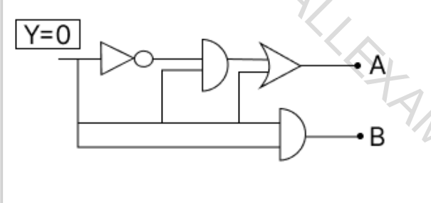
A=0, B=0
A=1, B=0
A=0, B=1
A=1, B=1
A=0, B=0
Given the input Y=0, the NOT gate outputs 1. This 1 is sent to an AND gate along with the original 0 (since Y=0), resulting in 1⋅0=0. Finally, the OR gate receives this 0 and another 0 from the input branch, resulting in 0+0=0 for output A, and the final AND gate receives 0 and 0, resulting in 0 for output B.
Given the input Y=0, the NOT gate outputs 1. This 1 is sent to an AND gate along with the original 0 (since Y=0), resulting in 1⋅0=0. Finally, the OR gate receives this 0 and another 0 from the input branch, resulting in 0+0=0 for output A, and the final AND gate receives 0 and 0, resulting in 0 for output B.
Think of a safety system: if the 'power off' switch is ON, the machine is disabled regardless of other conditions, similar to how the input 0 forces the final AND gate to output 0.
YNOT=Y — Inversion logic
YAND=A⋅B — AND logic
YOR=A+B — OR logic
Logic gates process binary signals based on Boolean algebra. An inverter (NOT gate) flips a signal (0 to 1), an AND gate outputs 1 only if all inputs are 1, and an OR gate outputs 1 if at least one input is 1. Following the signal path: NOT(0) = 1, AND(1,0) = 0, OR(0,0) = 0 (for A), and AND(0,0) = 0 (for B).
A NOT gate performs logical negation.
An AND gate outputs 1 only when all inputs are 1.
An OR gate outputs 0 only when all inputs are 0.
Digital Circuit Design
Microprocessor logic
Input Y=0.
Logic for A: (NOT(0)⋅0)+0=(1⋅0)+0=0+0=0.
Logic for B: 0⋅0=0.
A is correct — The signal propagation through the logic circuit starting with 0 results in both outputs A and B being 0.
Always trace the signal through each gate step-by-step; never assume a value without calculating the output of each gate stage.
Get instant step-by-step AI explanations, full shift Previous Year Papers (SSC GD, RRB, SSC JE), and regional rank analysis on the official Examoogle App.
 Free Download • 100K+ Aspirants